Board design
Building on Week 06's breakout board design for XIAO RP2040. Made the board square, with rounded corners, and only one button.
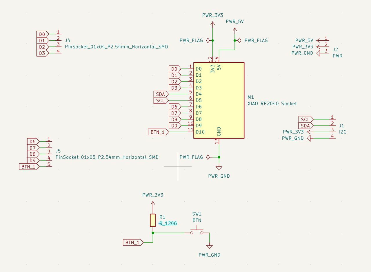
KiCAD schematic.
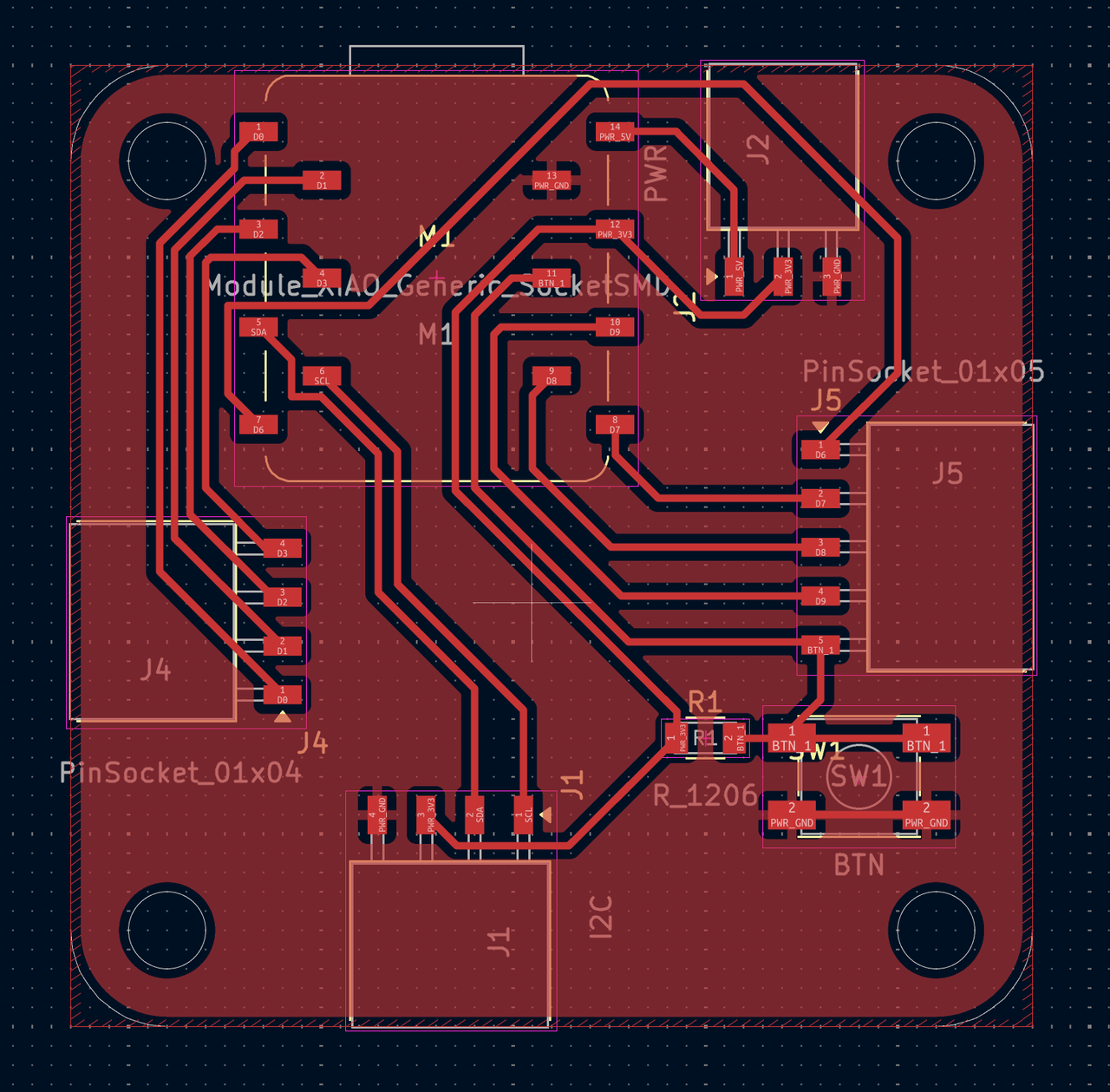
KiCAD PCB design.
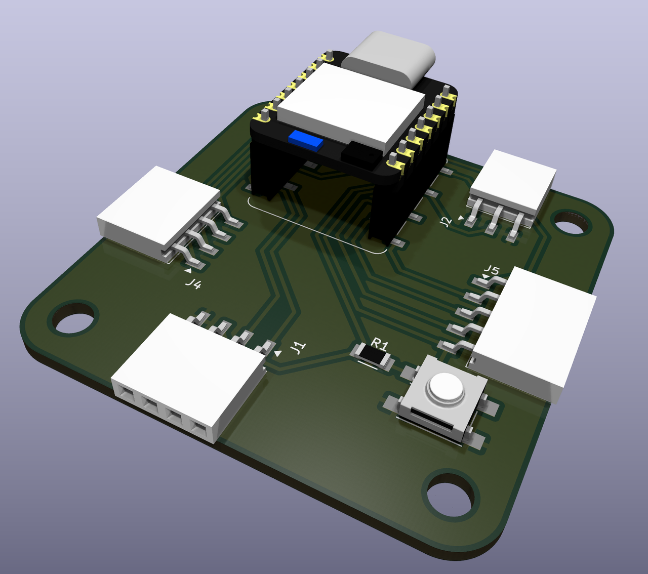
KiCAD 3D board view.
Board production
Using Bumgard CCD/2 mill and CopperCAM.
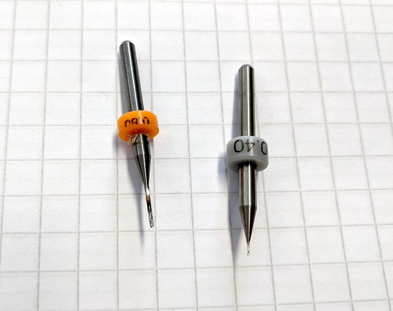
0.8mm and 0.4mm tools. The smaller is for engraving around the traces, and the larger is for cutting the edges.
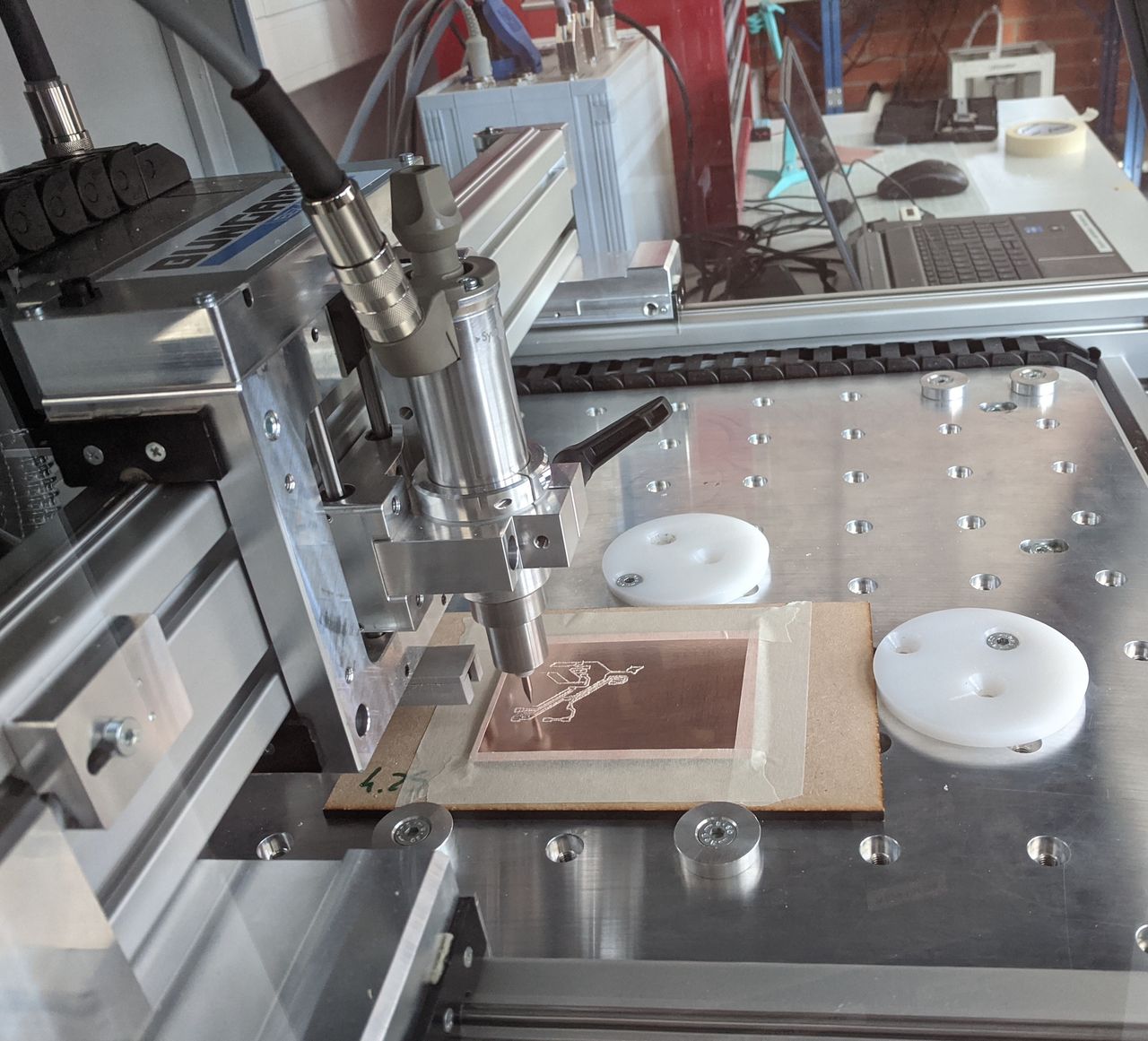
Bumgard mill working on a board.
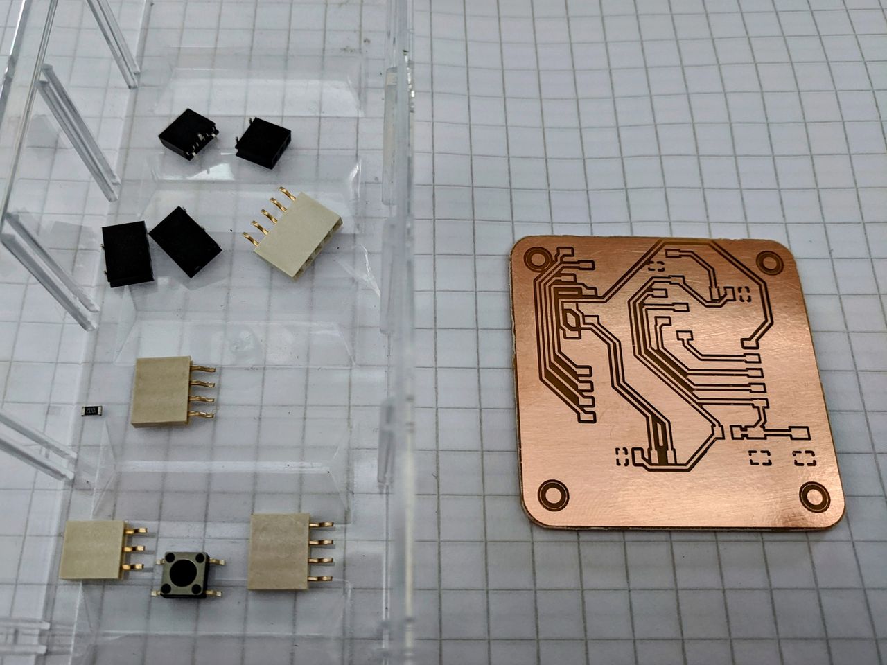
Completed board, and components selected.
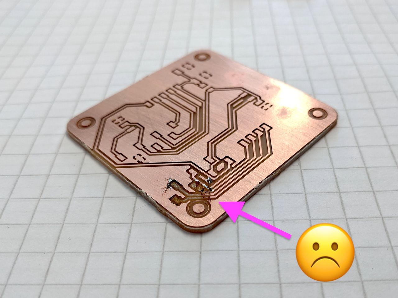
While soldering the first part, I made a bridge from the tab to the ground. I tried to remove it with copper braid, but I ended up pulling up the traces. Frustrating.
On the second board I used a box cutter to cut the accidental solder bridges. (This was a mistake, as some of the parts broke off with a little pressure. I have had better results clearing solder bridges with by melting the solder bridge and scraping the blob with the sodlering iron.)
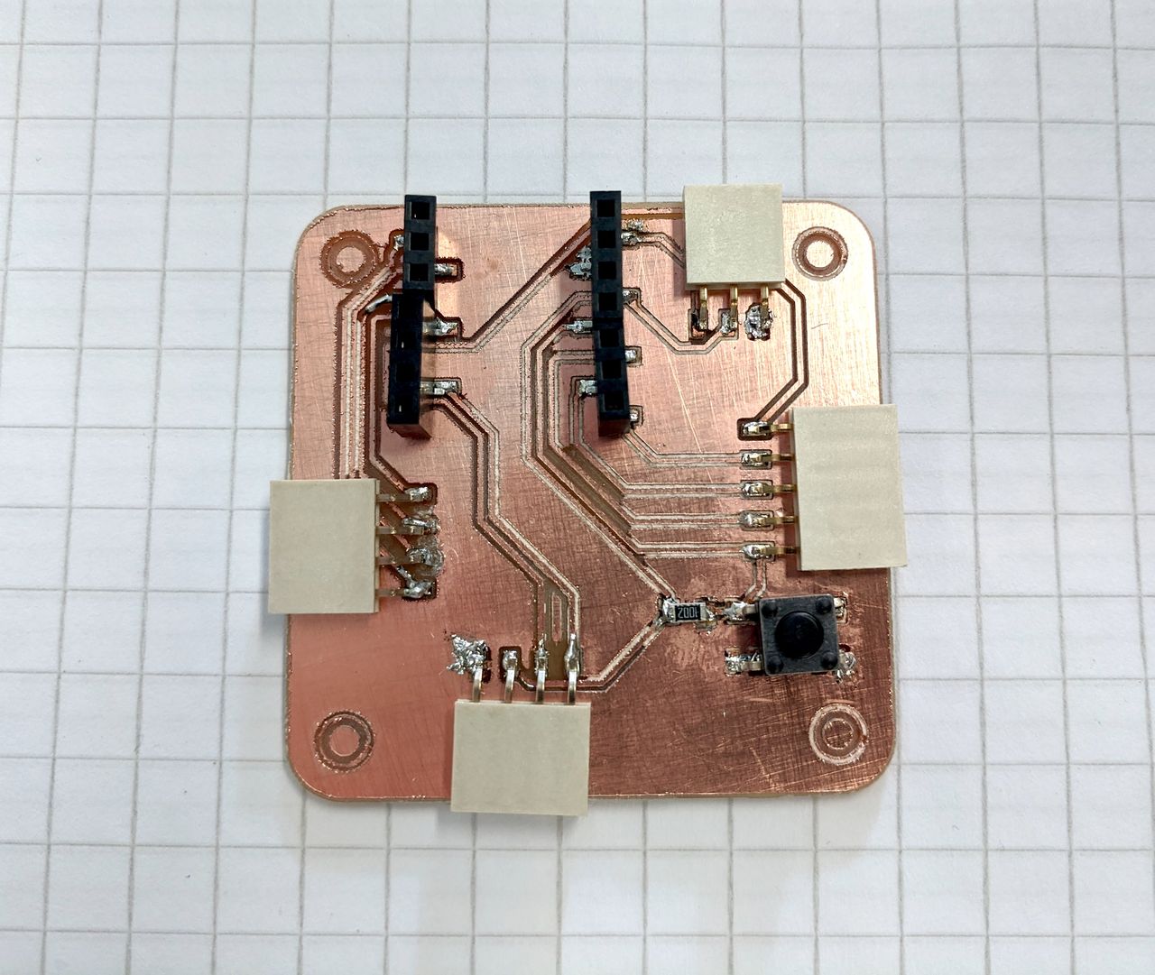
🥴
Everything connects where it should and there are no shorts. Room for improvement with the soldering.
There was a noticable difference in the trace quality between my two attempts today. For example, the burring along the traces, and dust that didn't clear in the path. Perhaps the tool used for the first one is newer.
v3
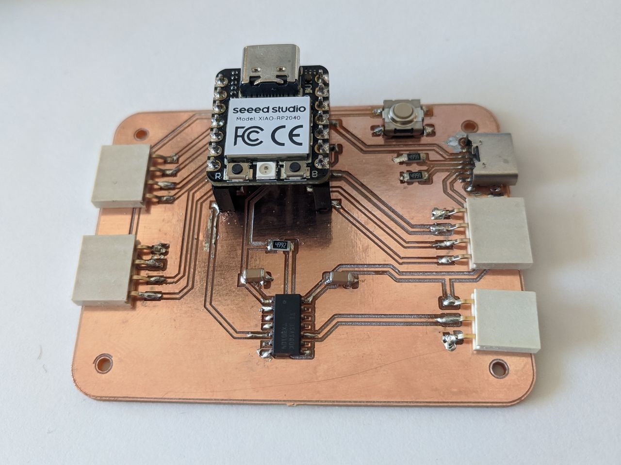
An improved attempt in week 10.
Future steps
- Look at tools under microscope, try to see difference.
- Get better at soldering.
- Try the hotplate or oven or hot air method.
- Connect with I2C sensor breakout boards.
- Figure out the design / CAM issue with the corner holes.
Project files
Reference
- Last year's group work
- Aalto wiki (Bumgard machine process needs to be added.)